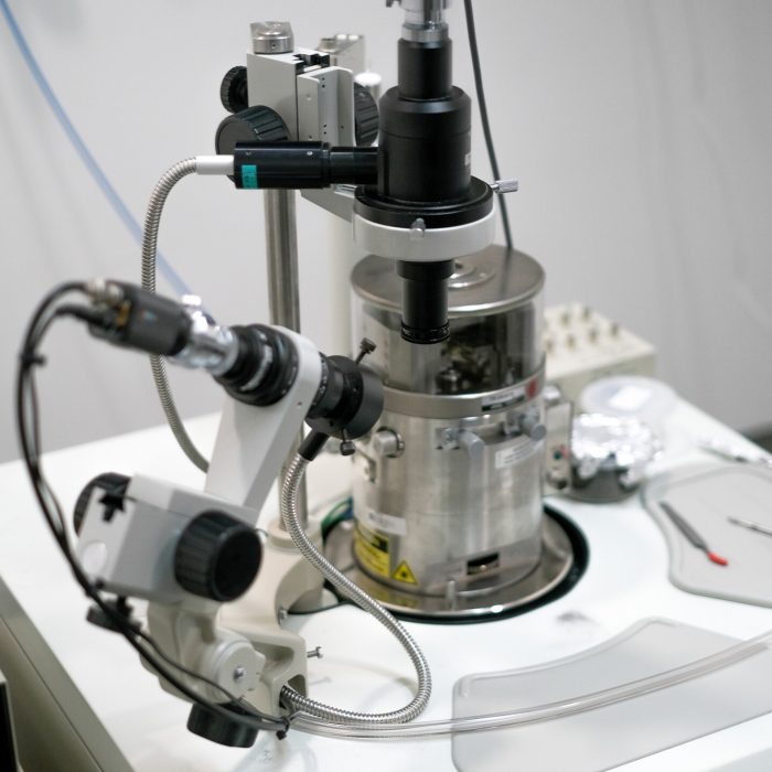
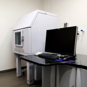
JEOL JSPM 5400 MkII Environmental SPM

Description
The JEOL 5400 MkII Environmental Scanning Probe Microscope (SPM) is a versatile and powerful instrument designed for high-resolution imaging and surface analysis of specimens at the nanoscale. It features a number of piezo-scanners and a range of atomic force microscopy imaging modes which may be operated in ambient or high-vacuum conditions (~10-4 Pa, sample permitting), enabling control of environmental conditions (pressure and temperature) during imaging. It is widely used in fields such as materials science and chemical for studying the topography and physical properties of different surfaces, especially thin films and 2D materials
Specifications
-
- Small sample holder, up to 15 by 15mm.
- Maximum sample height is 4mm
-
- Vertical resolution (z-axis) is 0.5nm or better
- Lateral resolution (x-y axis), depends on the types of AFM probe, typically around 3-5nm
- Pseudo atomic resolution possible in STM mode, sample permitting
- Maximum scan size is 20 by 20um for standard scanner, 150 by 150um for wide scanner.
- Z range is ± 2µm for standard scanner, ± 6µm for Z scanner and ± 4.5µm for wide scanner.
-
- Contact and tapping mode
- Non-contact and phase mode
- Conductive AFM (CAFM)
- Magnetic Force Microscopy (MFM)
- Vacuum and low temperature mode
- Scanning tunnel (STM)
Publishing Microscopy Data Acquired on the Joel JSPM 5400 MkII Enviromental SPM
-
-
- Type of samples: thin film or bulk material
- Processing methods/heat treatment for the thin film or bulk sample
- How sample is mounted, glued to a holder or soldered with indium
-
- Manufacturer: Joel
- Model: JSPM 5400 MkII Environmental SPM
-
- Type of measurement: AC mode, non-contact, contact mode
- Any advanced modes used: CAFM, MFM, LFM or vacuum mode · Scan size, scan rate, resolution
- Feedback setting, force set point, feedback gain
-
- Software used, Gwyddion (version) or Win SPMII
-
- Scalebar can be added using the AFM data processing software. X-Y scale bar can be added as a ruler to show the scan size or added as a traditional scale bar. The Z axis scale bar is added as a false colour bar.
Acknowledgement:
“The authors acknowledge the facilities and the scientific and technical assistance of Microscopy Australia at the Electron Microscope Unit (EMU) within the Mark Wainwright Analytical Centre (MWAC) at UNSW Sydney.”
Credit EMU staff: Feel free to mention EMU staff who have assisted you with your work! If staff have been involved with your work beyond basic training and support (e.g., project design, complex data/image processing, independent imaging/analysis, manuscript preparation), it may be appropriate to discuss co-authorship with the relevant staff and your supervisor.
Don’t forget to email the EMU lab manager with a copy of your publication to claim 2 hours of free microscopy time.
-
Applications
- Materials Science
- Semi-conductors
- Solar and battery materials
- Medical Sciences
Capabilities
Atomic force microscopy (AFM)
Surface roughness
Magnetic force microscopy
Instrument location
Electron Microscope Unit
B71, Basement
June Griffith Building (F10)
UNSW Sydney, NSW 2052
Access – To discuss training or how your project could benefit from using this microscope, please contact the EMU using the enquiries form or email EMUAdmin@unsw.edu.au
Parent facility
Explore more instruments, facilities & services
Our infrastructure and expertise are accessible to UNSW students and staff, external researchers, government, and industry.


