New FLEET publication on single-crystal technology for nano-scale devices
Published on the 20 August 2021

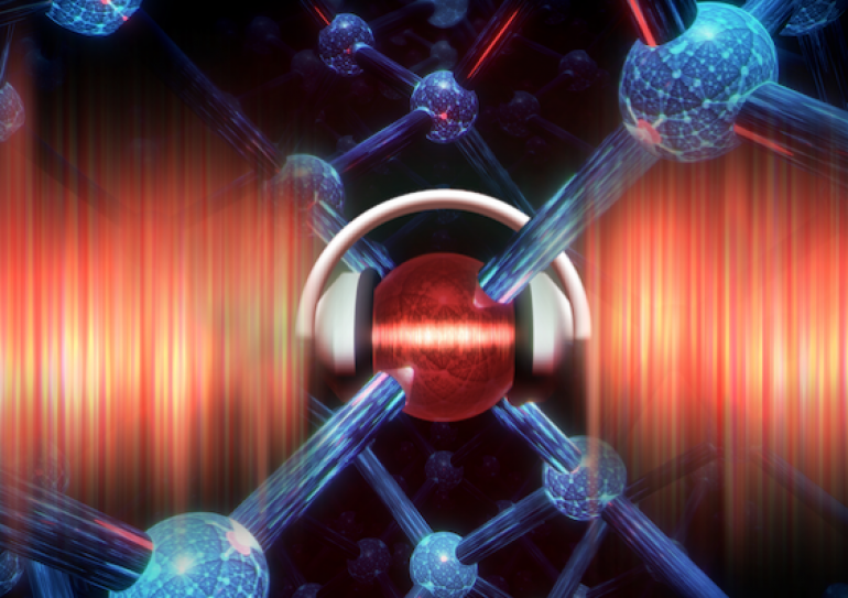
In a new publication, physicists from UNSW FLEET offer insights into the role charge noise plays in modern electronics and a single-crystal design for nano-scale devices.
The paper - The mobility of the two-dimensional electron gas (2DEG) in shallow GaAs/AlxGa1−xAsAlxGa1−xAsheterostructures – published in Applied Physics Letters, aims to better understand electronic performance in material structures.
Researchers Yonatan Ashlea Alava, Daisy Wang, Oleh Klochan, and Alex Hamilton (all from the School of Physics, UNSW), along with David Ritchie and Chong Chen (both from the University of Cambridge, Robinson College) examine the mobility of the two-dimensional electron gas (2DEG) in shallow GaAs/AlxGa1−xAsAlxGa1−xAsheterostructures. The outcomes of their research demonstrates that mobility is strongly suppressed by unwanted Coulomb scattering from surface charge, likely located in native surface oxides that form after the wafer is removed from the crystal growth system.
In addition, researchers showed that this native surface oxide can be eliminated by growing an epitaxial aluminum gate before removing the wafer from the growth chamber. The researchers fabricated accumulation mode devices on two wafers with nearly identical structures and growth conditions: one with an epitaxial aluminum gate 35 nm above the channel and another with an ex situ metal gate deposited on an aluminum oxide dielectric.
According to UNSW School of Physics PhD, Yonatan Alava, “Low temperature transport measurements show that the epitaxial gate design greatly reduces surface charge scattering, with up to 2.5×2.5× increase in mobility. Despite the ultra-shallow 2DEG (35 nm), the mobility remains high even at low carrier densities.”
FLEET scientists believe that the epitaxial aluminum gate can be patterned to make nanostructures by fabricating a quantum point contact that shows robust and reproducible 1D conductance quantization, with extremely low charge noise.
The authors gratefully acknowledge Richard Webster for the TEM measurements at the Mark Wainwright Analytical Centre, UNSW. They thank Asbjørn Drachmann for many helpful conversations. Device fabrication was carried out in part at the Australian National Fabrication Facility (ANFF) at the UNSW node. This work was funded by the ARC Centre of Excellence for Future Low Energy Electronics Technologies (No. CE170100039), and Non-Ergodic Quantum Manipulation, UK (No. EP/R029075/1).