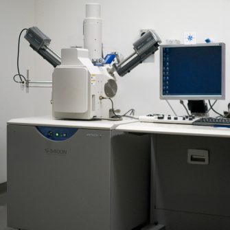
FEI Nova NanoSEM 230

Description
The NanoSEM 230 is a field-emission scanning electron microscope (FE-SEM), which attains ultra-high imaging resolution without the specimen size restrictions of a conventional in-lens FE-SEM due to the advanced design of the electron optics. The NanoSEM 230’s Schottky field-emission source allows the user to achieve high imaging resolution at a range of kV, at both low (high-resolution imaging) and high (microanalytical imaging) currents. Secondary electron (SE) imaging can be undertaken in both field-free and immersion mode for comprehensive low-to-high resolution imaging of a variety of samples. The NanoSEM 230 is fitted with a retractable four quad backscattered electron detector as well as an Oxford silicon drift detector energy dispersive X-ray spectroscopy (SDD-EDS) system for the convenient visualisation of compositional differences across the specimen surface.
Specifications
-
- Schottky field-emission electron gun 50V-30kV operating voltage
-
- 1nm at 15kV, 1.4nm at 1kV
-
- 2nm at 15kV
-
- In lens secondary election detector
- Everhart–Thornley secondary electron detector
- Four quad backscattered electron detector
-
- 20 mm2 Oxford X-ray energy dispersive spectroscopy (EDS)
-
- SEM pin stub holder
- Cross section holder
- Wafer holder
Publishing Microscopy Data Acquired on the FEI Nova NanoSEM 230
-
-
- Chemical fixation, dehydration, critical point drying
- Mounting in resin
- Staining
- Polishing
- Mounting on stub with adhesive
- Coating
-
- Manufacturer: FEI
- Model: Nova NanoSEM 230
- Type: Schottky FEG
-
- Accelerating voltage (kV)
- Detector(s) used for imaging (SE, BSE, EBSD, SDD-EDX)
-
- Detector: Oxford X-Max 20mm2 EDS detector
- Software: Oxford AZtec
- Accelerating voltage (kV)
- For quantitative analysis: matrix correction used, calibration method used (standardless or specify standards), elements calculated via difference or stoichiometry, excluded elements, accuracy of elemental values as shown by measurement of standard(s) of known composition
-
- Adjustments to contrast/brightness
- EDS map filters applied
-
- Scalebars can be added or removed from images in the export options.
Acknowledgement:
“The authors acknowledge the facilities and the scientific and technical assistance of Microscopy Australia at the Electron Microscope Unit (EMU) within the Mark Wainwright Analytical Centre (MWAC) at UNSW Sydney.”
Credit EMU staff: Feel free to mention EMU staff who have assisted you with your work! If staff have been involved with your work beyond basic training and support (e.g., project design, complex data/image processing, independent imaging/analysis, manuscript preparation), it may be appropriate to discuss co-authorship with the relevant staff and your supervisor.
Don’t forget to email the EMU lab manager with a copy of your publication to claim 2 hours of free microscopy time.
-
Applications
- Materials Science
- Life sciences
- Biomaterials
- Solar and battery materials
- Earth Sciences
- Medical Sciences
Capabilities
- Secondary electron imaging
- Backscatter imaging
- Energy dispersive X-ray analysis (EDX)
Instrument location
Electron Microscope Unit
B67, Basement
June Griffith Building (F10)
UNSW Sydney, NSW 2052
Access – To discuss training or how your project could benefit from using this microscope, please contact the EMU using the enquiries form or email EMUAdmin@unsw.edu.au
Parent facility
Explore more instruments, facilities & services
Our infrastructure and expertise are accessible to UNSW students and staff, external researchers, government, and industry.


