TEM - JEOL F200 (Hilmer)
Versatile Transmission Electron Microscope for high-resolution imaging, diffraction, and elemental analysis of advanced materials

Description
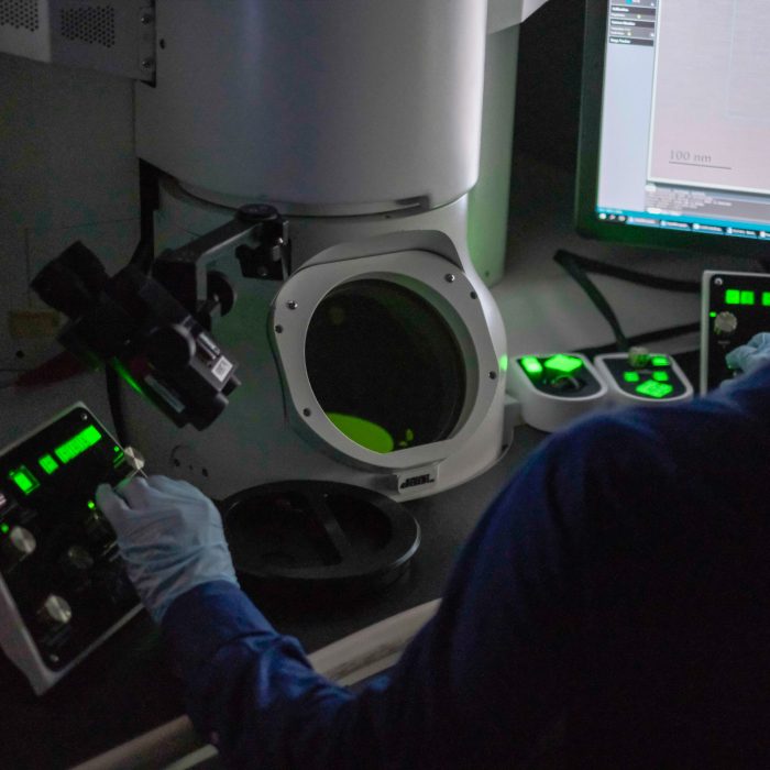
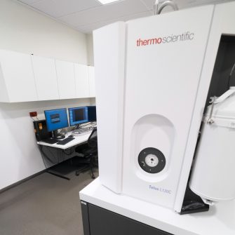
The JEM-F200 in E10 is high-resolution analytical (scanning) transmission electron microscope (S/TEM). This microscope has a high brightness cold-field emission gun capable of imaging atomic structures (HRTEM), electron diffraction and fast chemical elemental mapping using X-ray energy dispersive Spectroscopy (XEDS). Additionally, this microscope is specially configured for in-situ S/TEM imaging and 4D-STEM utilising our range of in-situ holders and high speed in-situ movie recording camera.
Specifications
-
Cold field-emission electron gun 80-200 kV operating voltage with <0.35 eV energy spread
-
0.1 nm (lattice resolution) at 200kV
-
0.16 nm (lattice resolution) at 200kV
-
- Gatan OneView IS camera (25 fps @ 4k x 4k) capable of in-situ TEM and 4D-STEM
- JEOL ADF and BF STEM detectors
-
- 100 mm2 JEOL X-ray energy-dispersive spectroscopy (XEDS), with a collection angle of 0.9 steradian.
-
- JEOL Low Background Double Tilt Holders
- JEOL Single Tilt Holders
- JEOL High Tilt Holders (± 80°) (for Tomography)
- Hummingbird 9 contact Heating and Biasing
- Hummingbird Liquid Flow cell
- Hummingbird Gas heating holder
- Protochips Atmosphere in-situ holder
- Simple Origin cryo-transfer holder
- Fischione Gas/Vacuum transfer holder
Publishing Microscopy Data Acquired on the TEM - JEOL F200 (Hilmer)
-
-
- Drop cast nanoparticles
- Ga or plasma FIB details
- Mechanical Polishing etc.
-
- Manufacturer: JEOL
- Model: JEM-F200
- Type: Transmission Electron Microscope (S/TEM)
-
- Accelerating voltage (80 or 200 kV)
- Detector(s) used for imaging
-
- Scalebars can be added or removed from images in the export options.
Acknowledgement:
“The authors acknowledge the facilities and the scientific and technical assistance of Microscopy Australia at the Electron Microscope Unit (EMU) within the Mark Wainwright Analytical Centre (MWAC) at UNSW Sydney.”
Credit EMU staff: Feel free to mention EMU staff who have assisted you with your work! If staff have been involved with your work beyond basic training and support (e.g., project design, complex data/image processing, independent imaging/analysis, manuscript preparation), it may be appropriate to discuss co-authorship with the relevant staff and your supervisor.
Don’t forget to email the EMU lab manager with a copy of your publication to claim 2 hours of free microscopy time.
-
Applications
- Materials Science
- Semi-conductors
- Solar and battery materials
- Medical Sciences
Capabilities
- High Resolution TEM (HRTEM)
- Dark Field TEM (DF-TEM)
- Electron Diffraction
- Beam-sensitive material
High-angle annular dark field STEM (HAADF)
- Annular bright field STEM (ABF)
4D-STEM
Lorentz TEM
Elemental mapping
X-ray Energy Dispersive Spectroscopy (XEDS, EDS, EDX)
3D electron tomography
In-situ: movie capture, heating biasing, gas heating, liquid flow
Instrument location
Electron Microscope Unit
B22a, Basement
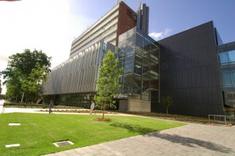
Hilmer Building (E10)
UNSW Sydney, NSW 2052
Access – To discuss training or how your project could benefit from using this microscope, please contact the EMU using the enquiries form or email EMUAdmin@unsw.edu.au
Parent facility
Explore more instruments, facilities & services
Our infrastructure and expertise are accessible to UNSW students and staff, external researchers, government, and industry.


.cropimg.width=335.png)


