
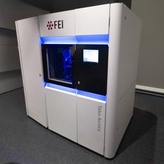
FIB - Zeiss Crossbeam 550 Cryo-FIB
A powerful tool for lamella sample preparation in both material science and frozen-hydrated biological samples.

Description
The Zeiss Crossbeam 550 focused ion beam scanning electron microscope (FIB-SEM) is a highly versatile instrument that combines high-resolution SEM imaging with advanced FIB capabilities, enabling TEM lamella preparation, nanofabrication, and 3D analysis for material and life sciences.
Materials Science
The Crossbeam 550 consists of a Gemini 2 SEM and the new Ion-sculptor Ga-FIB column, with platinum and carbon gas injection systems for in-situ deposition. This Ga-based FIB is a powerful platform for site-specific 2D and 3D analytical applications. Combining SmartFIB with advanced drift correction enables sophisticated stage motion control for automatic milling and serial data collection from multiple regions of interest. This provides a user-friendly workflow for nanofabrication, cross-sectional milling and imaging, and fabrication of ultrathin lamellae for further TEM analysis. The Crossbeam 550 is also equipped with an Oxford Ultim Max 170 silicon drift detector energy dispersive X-ray spectroscopy (SDD EDS) system, which enables simultaneous data collection with high-resolution elemental analysis and imaging capabilities. The Atlas 5 software package provides an advanced design programming environment for nanofabrication and 3D EDS volume imaging.
Life Science
The Crossbeam 550 is equipped with a Quorum cryo-stage and cryo-transfer system, which facilitates serial block face imaging and TEM lamella preparation from cells or tissues for high-resolution cryo-TEM imaging at cryogenic temperatures. The instrument also supports cryo-SEM imaging, TEM lamella preparation and 3D volume imaging for plastic-embedded tissue blocks. It can also be used with our correlative cryogenic workflow, consisting of a Linkam Scientific cryo-stage (CMS196), confocal LM (ZEISS LSM900 with Airyscan) and ZEN Connect software. This enables a seamless correlative cryo workflow that connects various microscopy techniques between cryo light microscopy, cryo-FIB, and cryo-TEM.
Specifications
-
- Electron Source Filament: Schottky field emitter
- Resolution (max. probe current 40 nA):
- 0.6 nm at 30 kV (STEM mode)
- 0.7 nm at 15 kV*
- 1.4 nm at 1 kV *
- Analytical Condition (10 nA, WD 5 mm): 2.3 nm at 20 kV
- Acceleration Voltage: 0.02 - 30 kV (SEM)
- Magnification Range: 12x - 2,000,000x (SEM)
-
- Ion Source Type: UHV, with Gallium liquid metal ion source (Ga-LMIS)
- FIB resolution: 3nm at 30kV, 120nm at 1kV, 330nm at 500V
- Acceleration Voltage: 0.5 – 30 kV
- Magnification: 300x - 500,000x
- Probe Current: 1 pA to 100 nA
-
- The angle between SEM column and FIB column is 54 degrees.
- EDS Take-off Angle: 35 degrees
-
- UniGIS Injector Heating: Reservoir heating temperature 30 to 90 °C
- Available Precursor Materials: Pt, C
-
Sample manipulation in preparation chamber
- Sputter coating with Platinum in Argon atmosphere
- Sample sublimation
- Control of temperature by built-in heater
- Sample fracture with built-in knife
Minimum temperatures:
- Rotate stage SEM: down to –175°C
- Anti-contaminator (SEM): down to –190°C
- Stage (preparation chamber): down to –190°C
- Anti-contaminator (preparation chamber): down to –190°C
- Stability of temperatures: < 0.5 °C
Publishing microscopy data acquired on the Zeiss Crossbeam 550 Cryo-FIB-SEM
-
-
- Manufacturer: Zeiss
- Model: Crossbeam 550 Cryo-FIB SEM
- Type: Schottky Feild Emission
Acknowledgement:
“The authors acknowledge the facilities and the scientific and technical assistance of Microscopy Australia at the Electron Microscope Unit (EMU) within the Mark Wainwright Analytical Centre (MWAC) at UNSW Sydney.”
Credit EMU staff: Feel free to mention EMU staff who have assisted you with your work! If staff have been involved with your work beyond basic training and support (e.g., project design, complex data/image processing, independent imaging/analysis, manuscript preparation), it may be appropriate to discuss co-authorship with the relevant staff and your supervisor.
Don’t forget to email the EMU lab manager with a copy of your publication to claim 2 hours of free microscopy time.
-
Applications
- Life sciences
- Biomaterials
- Medical Sciences
- Materials Science
- Solar and battery materials
- Earth Sciences
Capabilities
TEM lamella preparation for material and biological samples
3D volume imaging for material and biological samples
Backscatter imaging
Energy dispersive X-ray analysis (EDX)
Topography
Funding partners


Instrument location
Electron Microscope Unit
Room B04
Science and Engineering Building (E8)
UNSW Sydney, NSW, 2052
Access – To discuss training or how your project could benefit from using this microscope, please contact the EMU using the enquiries form or email EMUAdmin@unsw.edu.au
Parent facility

Explore more instruments, facilities & services
Our infrastructure and expertise are accessible to UNSW students and staff, external researchers, government, and industry.