FIB – Thermo Scientific Helios G5 PFIB UXe

Description
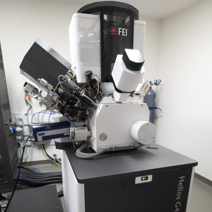
The FIB – Thermo Scientific™ Helios™ G5 PFIB UXe is an advanced analytical platform for multi-disciplinary applications on large volume 3D characterization, Ga+ free sample preparation and precise micromachining.
The Helios G5 PFIB UXe DualBeam system incorporates a new generation of 2.5 µA Xe plasma focused ion beam (PFIB) column and ultrahigh resolution monochromator scanning electron column. It provides unique and fast ion milling capabilities with 50x higher throughput milling rate (compared to that in a Ga-based FIB), and rapid cross-sectioning of features up to 900 µm . It can deposit patterned conductors, e.g. C, W and Pt, and selectively etch semiconductor devices with delineation agent TFA. It equipped with an Easylift micromanipulator for in-situ lift-out process. It can achieve the reliable and repeatable long term 3D data acquisition with a unique 6” piezo stage. It is designed for high throughput, large volume processing, combined with extreme high-resolution imaging in both 2D and 3D for advanced materials characterization.
This PFIB has also extended 3D analytical capabilities including electron backscatter diffraction (EBSD) and electron dispersive X-ray spectroscopy (EDS). Oxford Aztec Symmetry EBSD system is an integrated EBSD data collection and analysis system based on a CMOS detector with ForeScatter Electron (FSE) imaging functions, providing ultra-high speed data acquisition at over 3000 indexed patterns per second (pps). The Oxford Ultim Max 170 silicon drift detector (SDD EDS) system is the most sensitive system currently available for high-speed elemental X-ray microanalysis. This large area SDD provides a very high collection efficiency benefitting speed, sensitivity, and analytical spatial resolution. Simultaneous data collection can be used in phase identification where the X-ray data is used to identify candidate phases and the EBSD data used to distinguish the phases.
Specifications
-
- Extreme high-resolution field emission Elstar SEM Column with: – Magnetic immersion objective lens– High-stability Schottky field emission gun to provide stable high-resolution analytical currents– UC+ monochromator technology
- SmartAlign: user-alignment-free technology
- 60-degree dual objective lens with pole piece protection allows tilting larger samples
- Automated heated apertures to ensure cleanliness and touch free aperture exchange
- Electrostatic scanning for higher deflection linearity and speed
- Thermo Scientific ConstantPower™ Lens Technology for higher thermal stability
- Integrated Fast Beam Blanker*
- Beam deceleration with stage bias from 0 V to -4 kV*
- Minimum source lifetime: 12 months
-
- At optimum WD: – 0.7 nm at 1 kV– 1.0 nm at 500 V (ICD)
- At coincident point: – 0.6 nm at 15 kV– 1.2 nm at 1 kV Electron beam parameter space
- Electron beam current range: 0.8 pA to 100 nA
- Accelerating voltage range: 350 V – 30 kV
- Landing energy range: 20* eV – 30 keV
- Maximum horizontal field width: 2.3 mm at 4 mm WD
-
- High-performance PFIB column with Inductively coupled Xe+ Plasma (ICP)
- Ion beam current range: 1.5 pA to 2.5 µA
- Accelerating voltage range: 500 V - 30 kV
- Maximum horizontal field width: 0.9mm at beam coincidence point Ion beam resolution at coincident point
- <20 nm at 30 kV using preferred statistical method
- <10 nm at 30 kV using selective edge Method
-
High precision 5-axis motorized stage, with XYR axis piezo driven
- XY range: 150 mm
- Z range: 10 mm
- Rotation: 360° (endless)
- Tilt range: -10° to +60°
- XY repeatability: 1 μm
- Max sample height: Clearance 55 mm to eucentric point
- Max sample weight at 0° tilt: 500 g (including sample holder)
- Max sample size: 150 mm with full rotation (larger samples possible with limited rotation)
- Compucentric rotation and tilt
-
- Complete oil-free vacuum system
- Chamber vacuum: <2.6×10⁻⁶ mbar (after 24 h pumping)
- Evacuation time: <5 minutes
-
- E- and I-beam coincidence point at analytical WD (4 mm SEM)
- Ports: 21
- Inside width: 379 mm
- Integrated plasma cleaner
-
- Dwell time range from 25 ns – 25 ms/ pixel
- Up to 6144 × 4096 pixels
- File type: TIFF (8, 16, 24-bit), BMP or JPEG standard
- SmartSCAN (256 frame average or integration, line integration and averaging, interlaced scanning)
- DCFI (Drift Compensated Frame Integration)
Publishing Microscopy Data Acquired on the Thermo Scientific Helios G5 PFIB UXe
-
-
- Chemical fixation, dehydration, critical point drying
- Mounting in resin
- Staining
- Polishing
- Mounting on stub with adhesive
- Coating
-
- Manufacturer: Thermo Scientific
- Model: Helios G5 PFIB UXe
- Type: Dualbeam PFIB-SEM
-
- Accelerating voltage (kV)
- Detector(s) used for imaging (SE, BSE, EBSD, SDD-EDX)
-
- Accelerating voltage (kV)
- Beam Current (nA)
- X-ray lines analysed
- Calibration method (standards, matrix correction)
- Elements calculated via difference or stoichiometry
- Accuracy of elemental values as shown by measurement of secondary standard(s) of known
- For quantitative analysis: matrix correction used, calibration method used (standardless or specify standards), elements calculated via difference or stoichiometry, excluded elements, accuracy of elemental values as shown by measurement of standard(s) of known composition
-
- Adjustments to contrast/brightness
- EDS map filters applied
-
- Scalebars can be added or removed from images in the export options.
Acknowledgement:
“The authors acknowledge the facilities and the scientific and technical assistance of Microscopy Australia at the Electron Microscope Unit (EMU) within the Mark Wainwright Analytical Centre (MWAC) at UNSW Sydney.”
Credit EMU staff: Feel free to mention EMU staff who have assisted you with your work! If staff have been involved with your work beyond basic training and support (e.g., project design, complex data/image processing, independent imaging/analysis, manuscript preparation), it may be appropriate to discuss co-authorship with the relevant staff and your supervisor.
Don’t forget to email the EMU lab manager with a copy of your publication to claim 2 hours of free microscopy time.
-
Applications
- Materials Science
- Solar and battery materials
- Mechanical Engineering
- Electrical and Telecommunication Engineering
- Life sciences
- Biomaterials
- Earth Sciences
- Medical Sciences
Capabilities
Ion milling
TEM lamella making
3D volume imaging
Cross sectional analysis
3D EBSD
SEM imaging
Backscatter imaging
Energy dispersive X-ray analysis (EDX)
Topography
Instrument location
Electron Microscope Unit
B80, Basement
June Griffith Building (F10)
UNSW Sydney, NSW 2052
Access – To discuss training or how your project could benefit from using this microscope, please contact the EMU using the enquiries form or email EMUAdmin@unsw.edu.au
Parent facility
Explore more instruments, facilities & services
Our infrastructure and expertise are accessible to UNSW students and staff, external researchers, government, and industry.


