
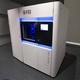
Zeiss Auriga Crossbeam FIB-SEM

Description
The Zeiss AURIGA® CrossBeam® Workstation (installed in 2011) is an analytical instrument that combines field emission (FE) SEM imaging with gallium and focused ion beam (Ga + FIB) capabilities, enabling cross sectional imaging, TEM lamella preparation, nanofabrication, and electron backscatter diffraction (EBSD) and a silicon drift detector energy dispersive X-ray spectroscopy (SSD-EDS) analyses for materials.
The Auriga FIB-SEM consists of a Gemini SEM column and the Canion Ga-FIB column, with platinum mono-gas injection systems for in-situ deposition, which provides a user-friendly workflow for cross-sectional milling and imaging, nanofabrication, and fabrication of thin lamellae for further TEM analysis. This Auriga FIB-SEM is also equipped with an Oxford X-Max 20 SDD EDS and Nordlys EBSD system, which enables simultaneous data collection with elemental analysis and EBSD mapping capabilities.
The AURIGA can be used to examine a wide range of dry and conductive specimens (coating prior to loading into the chamber is required for non-conductive materials). Its unique stage motion control system enables it to hold a wide range of sample sizes and to navigate between multiple indexed samples.
Specifications
-
- Electron Source Filament: Schottky field emitter
- Resolution: 1.0 nm at 15 kV, 1.9 nm at 1 kV
- Acceleration Voltage: 0.1 - 30 kV
- Probe current: 4 pA – 20 nA
- Magnification Range: 12x - 1,000,000x
-
- Ion Source Type: UHV, with Gallium liquid metal ion source (Ga-LMIS)
- FIB resolution: <7 nm at 30kV
- Acceleration Voltage: 5 – 30 kV
- Magnification: 300x - 500,000x
- Probe Current: 1 pA to 50 nA
-
- The angle between SEM column and FIB column is 54 degrees.
- EDS Take-off Angle: 35 degrees
-
- Pt
Publishing Microscopy Data Acquired on the Zeiss Auriga Crossbeam FIB-SEM
-
-
- Nanoparticle Drop-casting
- Chemical fixation, dehydration, critical point drying
- Mounting in resin
- Staining
- Ultramicrotomy
- TEM Grid details
-
- Manufacturer: Zeiss
- Model: Auriga Crossbeam
- Type: Schottky Feild Emission (FE)
-
- Accelerating voltage (kV)
- Detector(s) used for imaging
-
- Adjustments to contrast/brightness
-
- Scalebar can be added using the AFM data processing software. X-Y scale bar can be added as a ruler to show the scan size or added as a traditional scale bar. The Z axis scale bar is added as a false colour bar.
Acknowledgement:
“The authors acknowledge the facilities and the scientific and technical assistance of Microscopy Australia at the Electron Microscope Unit (EMU) within the Mark Wainwright Analytical Centre (MWAC) at UNSW Sydney.”
Credit EMU staff: Feel free to mention EMU staff who have assisted you with your work! If staff have been involved with your work beyond basic training and support (e.g., project design, complex data/image processing, independent imaging/analysis, manuscript preparation), it may be appropriate to discuss co-authorship with the relevant staff and your supervisor.
Don’t forget to email the EMU lab manager with a copy of your publication to claim 2 hours of free microscopy time.
-
Applications
- Materials Science
- Solar and battery materials
- Earth Sciences
Capabilities
TEM lamella preparation for solid material samples
3D volume imaging for material samples
Backscatter imaging
Energy dispersive X-ray analysis (EDX)
Electron Backscatter diffraction (EBSD)
Topography
Funding partners


Instrument location
Electron Microscope Unit
B74, Basement
June Griffith Building (F10)
UNSW Sydney, NSW 2052
Access – To discuss training or how your project could benefit from using this microscope, please contact the EMU using the enquiries form or email EMUAdmin@unsw.edu.au
Parent facility

Explore more instruments, facilities & services
Our infrastructure and expertise are accessible to UNSW students and staff, external researchers, government, and industry.